目录
印刷电路板(PCB)的历史
印刷电路板(PCB)的过去与现在
像历史上许多其他伟大的发明一样,我们今天所知道的印刷电路板(PCB)建立在历史进步的基础上。PCB的历史我们可以追溯到130多年前,在世界的某个角落,当时世界上最伟大的机器刚刚开始运转。我们将在这里介绍的内容并不是一个完整的历史,而是印刷电路板(PCB)怎样逐步变为今天的样子。
Why PCBs?
Over time, PCBs have evolved as a tool for optimizing the manufacturing of electronics. What was once assembled easily by hand soon gave way to microscopic components that required the precision and efficiency of machinery. Take for example the two circuit boards shown below. One is an older board for a calculator made in the 1960s. The other is a typical high density motherboard that you’ll see in computers today.
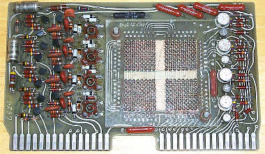
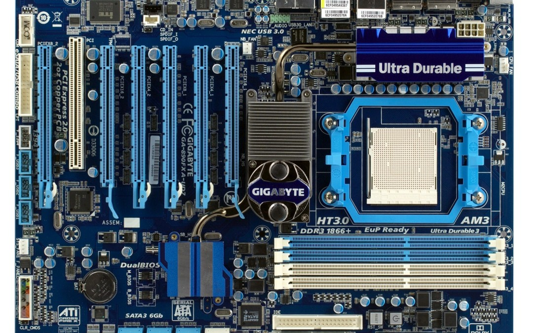
PCB comparison between a 1968 calculator and today’s modern motherboards.
In the calculator, we probably have 30+ transistors, but on a single chip on the motherboard, you’ll find over a million transistors. Point being, the rate at which technology and PCB design itself is advancing is impressive. Everything on that calculator PCB can now fit into a single chip on today’s designs. This brings to focus several noticeable trends in the manufacturing of PCBs:
- We are packing more functionality into advanced devices like integrated circuits (ICs) and microprocessors.
- We are shrinking passive components like resistors, capacitors, etc. to microscopic levels.
- All of this is leading to an increased density of components and complexity on our boards.
All of these advances are being driven primarily by the increased speed and functionality of our products. We expect our devices to respond instantly, and even a few seconds delay can send us into a frenzy. For functionality, think about video games. Back in the 80s, you were likely playing Pacman at the arcade. Now we’re seeing photorealistic representations of reality. The progress is just insane.

Video game visuals are nearly photorealistic these days.
It’s pretty clear to see that the evolution of PCBs is in direct response to our expectations from our devices. We demand faster, cheaper, more powerful products, and the only way to meet those needs is to miniaturize and make the manufacturing process more efficient. When did this whole craze for electronics and PCBs first begin? At the dawn of the Gilded Age.
The Gilded Age (1879 – 1900)
We’re out of the American Civil War in the 60s, and now manufacturing is booming in the United States. We’re making everything we can during this period, from food to clothing, furniture, and railroad tracks. The transportation industry was hammering away, and our greatest engineers were figuring out how to get someone from the east coast of the United States to the west coast in 5-7 days instead of 5-7 months.

The railroad made it possible to travel from the east to west coast in days, not months.
During this time we were also bringing electricity into households, first starting in cities, then moving into the suburbs and rural areas. Electricity was now an alternative for coal, wood, and oil. Think about living in New York in the dead of winter, trying to cook a meal or heat your home with dirty coal or stacks of firewood. Electricity changed all of this.
One interesting note is that Standard Oil, which had a monopoly on the oil market, wasn’t supplying oil for gasoline. Their market was oil burned for cooking, frying, and lighting. With electricity entering the picture, Standard Oil would need to define a new purpose for oil, which would arrive with the introduction of the automobile.

Shares of Standard Oil Company issues in May 1878, the beginning of the oil monopoly.
During the Gilded Age, we saw some major discoveries in electromagnetics. We have the invention of the motor, which converts electrical energy into mechanical energy. We also see generators, which do the opposite by converting mechanical energy into electrical energy.
This was also a period of genius inventors who still have an impact on our world of electronics today, including:
- Thomas Edison invented the lightbulb in 1879, movies in 1889, and many other innovations.
- Nikola Tesla invented the motor in 1888 and AC power in 1895.
- Alexander Graham Bell invented the telephone in 1876.
- George Eastman’s Kodak invented the first consumer camera in 1884.
- Herman Hollerith invented the tabulator in 1890 and would go on to found IBM.
One of the greatest debates during this intense period of innovation was between AC and DC. Tesla’s AC ended up winning out as an ideal method of transporting electricity over long distances. However, what’s interesting to note is how we’re still dealing with AC-DC conversion issues today.
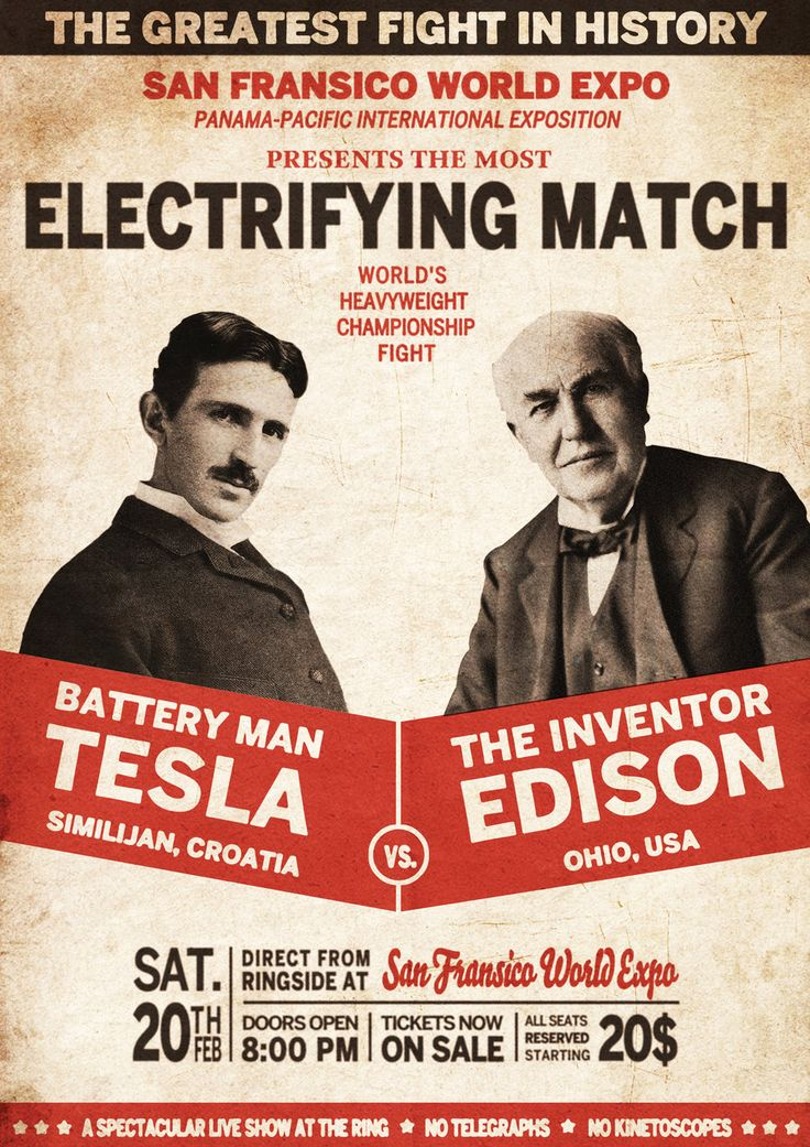
AC might have won the fight, but DC still dominates electronics.
Look at any electronic device that you plug into the wall, and you’ll need to convert the AC to DC. Or if you look at the infrastructure required for solar panels, they produce electricity in DC, which has to be turned back into AC for mains, and then back into DC to be used by our devices. You could almost say that the AC-DC debate never ended, a balance was just settled between two opposing ideas.
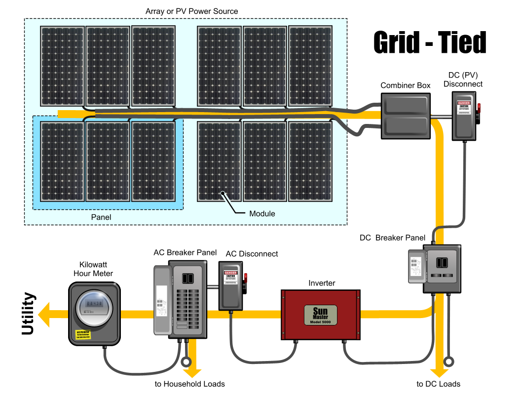
There’s a lot of back and forth between AC and DC in solar panels.
Note that the beginning ideas for the PCB were not invented during the Gilded Age. However, without the manufacturing prowess of this time, and the spreading influence of electricity, the PCB would never be what it is today.
The Progressive Era (1890 – 1920)
The Progressive Era was marked by a time of social reform, with legislation like the Sherman Antitrust Act which breaks up the monopoly of Standard Oil. This is also a time when we see the first patent for a PCB. In 1903, German Inventor Albert Hanson files a British patent for a device described as a flat, foil conductor on an insulating board with multiple layers. Sound familiar?

A drawing depicting the first PCB patent secured by Albert Hanson. (Image source)
Hanson also described the concept of a through-hole application in his patent. Here he showed that you could punch a hole through two layers that had perpendicular wires to establish electrical connectivity.
During this time we start to see a major push for electric-powered devices into everyday households by Edison and other business leaders. The problem with this push was the complete lack of standardization. If you lived in New York or New Jersey and used Edison’s electric inventions for lighting, heating, or cooking, what would happen if you used them in another city? They were unusable because each town had their own socket configurations.
This problem was also made worse by the fact that Edison didn’t just want to sell people a light bulb, he wanted to sell a service. You’d get your electric service hooked up by Edison for a monthly fee; then you’d buy the light bulbs, appliances, etc. Of course, none of these services were compatible with other competing methods.
We have Harvey Hubbel to thank for finally ending this mess. In 1915 he filed a patent for the standard wall outlet plug that is still in use today. Now we don’t have toasters or heating plates being plugged into light bulb sockets. It’s a massive win for standardization in the industry.
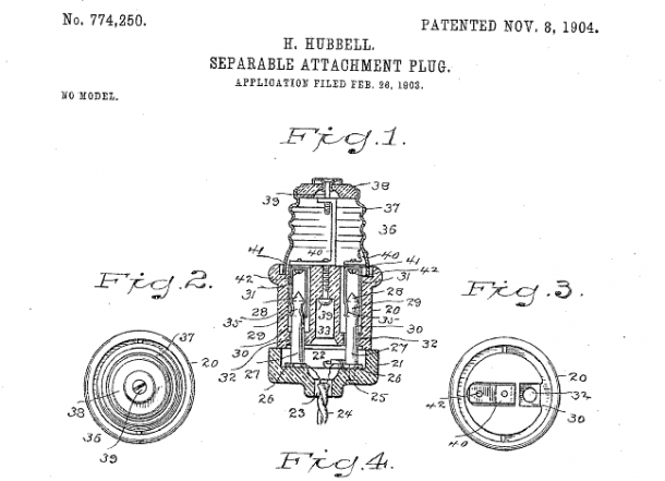
Thanks to Harvey Hubbel we now have a standardized wall outlet for all electronics.
One last thing to note is that the Progressive Era marked the first World War. This conflict was purely focused on mechanical devices and trench warfare. The PCB concept, and even basic electronics, still hadn’t come into use for military applications, but they soon would.
The Roaring Twenties (1920s)
With World War I coming to a close we’re now in the Roaring Twenties and seeing a giant economic boom in the United States. This was the first time in history that more people lived in cities than in farms. We’re also starting to see the introduction of chain stores and brands throughout the United States. You might have had one or two family-owned shops in two different towns, but now we have major brands and stores going national.
The greatest invention during this period was the automobile by Henry Ford and its required infrastructure. This situation is similar to the 1990s, where we had to build a major infrastructure to handle the internet and our information age by building switches, routers, and fiber optic cables. The automobile was no different.
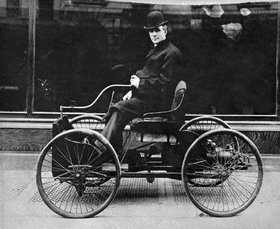
Henry Ford’s first car – the Quadricycle.
Here we see roads that were once mud being paved. People needed gasoline to power their vehicles, so gas stations arose. You’ve also got repair shops, accessories, etc. An entire way of life for many people was born out of the invention of the automobile, as it still is today.
It was also during this time that we saw the introduction of the modern appliances we still rely on today like washing machines, vacuums, and refrigerators. This was the first time that people were able to shop at the store for perishable goods and store them for prolonged freshness.
But where are our PCBs? We’re still not seeing them used in any of the appliances or automobiles introduced during this time. However, in 1925 Charles Ducas submitted a patent which describes the process for adding conductive inks to an insulating material. This would later give birth to the printed wiring board (PWB). This patent was the first real application to resemble a PCB but was only used as a flat heating coil. We still haven’t gotten to any actual electrical connectivity between board and components, but we’re getting close.
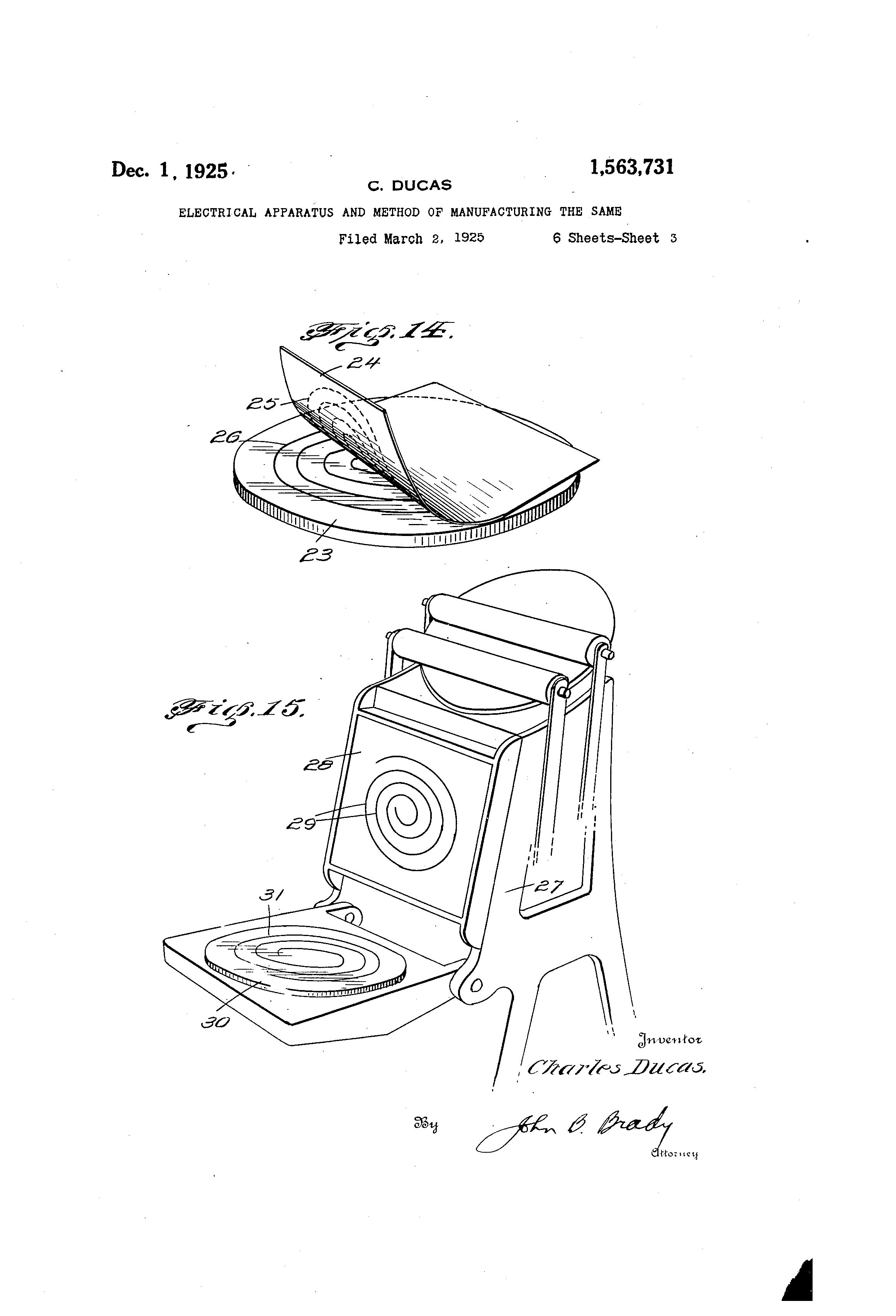
The PCB evolves, this time being used as a heating coil from Charles Ducas.
The Great Depression (the 1930s)
In 1929 the stock market plummeted and all of the great inventions at innovations of our time come tumbling down. Here we see a period of 25%+ unemployment, with 25,000 banks failing and a ton of hardship that ripples throughout the world. This was a miserable time for humanity as a whole and paved the way for the rise of Hitler, Mussolini, Stalin, and our future world conflict. PCBs might have laid quiet until now, but that was all about to change.
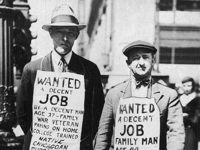
The great depression affected everyone, from banks to the average worker.
World War 2 (1939 – 1945)
The second World War is underway, and the United States enters the fray in 1942 after the bombing of Pearl Harbor. What’s interesting to note about Pearl Harbor is the entire failure in communication leading up to the attack. The United States had good evidence of an impending crisis, but all methods of communicating with their military base in Honolulu were unsuccessful, and so the island was caught by surprise.

A battleship lost in the attack on Pearl Harbor.
Because of this failure, the U.S. Department of Defense realized they needed a more reliable method of communication. This brought electronics to the forefront as a primary means of communication to replace morse code.
It was also during World War 2 that we saw the first use of a PCB as we know it today in the proximity fuse. This device was used for high-velocity artillery shells, which needed to fire precisely over massive distances in either sky or land. The proximity fuse was initially developed by the British to combat the push of Hitler’s Army. It was later shared with the United States who perfected the design and manufacturing.
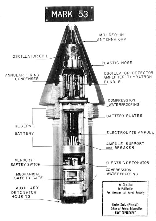
One of the first military applications to use a PCB – the proximity fuse.
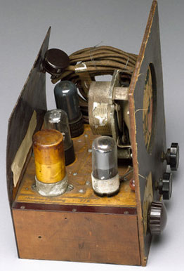
During this time we also have Paul Eisler, an Austrian living in the UK, file a patent for copper foil on a non-conductive base of glass. Sound familiar? This is the concept we still use today for manufacturing PCBs with an insulating layer and copper on the top/bottom. Eisler took this idea one step further by making a radio with his PCB in 1943, which would pave the way for future military applications.
A radio made by Paul Eisler with the first printed circuit board (PCB).
The Baby Boomers (the 1940s)
As World War 2 comes to a close, we see our soldiers arriving home, starting families, and having a ton of children. Cue the Baby Boomer generation. It’s during this Post War age where we see a ton of improvements to existing appliances like vacuum cleaners, washing machines, televisions, and radios. Now that the Great Depression has passed many consumers can finally afford these devices in their homes.
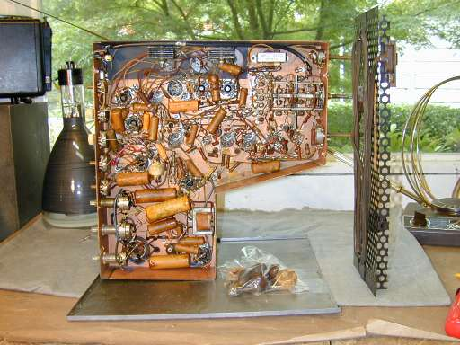
What we’re still not seeing though are consumer-level PCBs. Where is Paul Eisler’s work? Take a look at this old television below, and you’ll see all of the components but no underlying PCB foundation.
An old Motorola television from 1948 with no PCB.
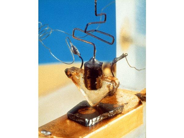
Despite the lack of PCBs, we did see the arrival of the transistor at Bell Labs in 1947. It took another six years in 1953 for this device to finally be used in products, but why so long? Back in those days, information was spread through journals, conferences, etc. The spread of information simply took time to travel before the Information Age.
The first transistor, born in Bell Labs in 1947.
The Cold War Era (1947 – 1991)
The Cold War Era arrives, marking a considerable period of tension between the United States and the Soviet Union. These two giants almost go to battle with each other and keep the world suspended in a threat of nuclear annihilation over the differences between capitalism and communism.
To stay ahead of this arms race, both sides had to beef up their communication abilities to understand what the enemy was doing. It’s here where we see PCBs being used to their full potential. In 1956 the United States Army released their patent for the “Processing of Assembling Electrical Circuits.” Now manufactures had a method to both hold electronics and establish connectivity between components with copper traces.
As PCBs start to kick off in the manufacturing realm, we find ourselves in the world’s first Space Race. Russia had some amazing accomplishments during this time, including:
- Launching the first satellite, Sputnik, in 1957
- Launching the first spacecraft, Luna 2, to the moon in 1959
- Sending the first cosmonaut, Yuri Gagarin, around the earth in 1961
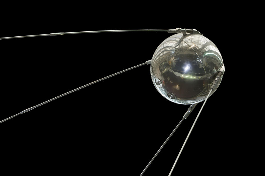 The first satellite, Sputnik, launched by Russia in 1957.
Where was the United States in all of this? Mainly falling behind, often taking a year or two to develop the same technologies. In response to this gap, we see the U.S. space budget increasing 5x in 1960. We also have the famous President Kennedy Speech in 1962, part of which deserves to be quoted below:
“We choose to go to the Moon! We choose to go to the Moon in this decade and do the other things, not because they are easy, but because they are hard; because that goal will serve to organize and measure the best of our energies and skills, because that challenge is one that we are willing to accept, one we are unwilling to postpone, and one we intend to win.” – U.S. President John F. Kennedy, September 12, 1962
All of this leads to a landmark moment in history. July 20, 1969, the United States lands the first man on the moon.

The first man on the moon, a historic moment for humanity.
Back to PCBs, in 1963 we have Hazeltyne Corporation filing a patent for the first plated through-hole technology. This would allow components to be closely spaced together on a PCB without worrying about crossover connections. We also see the introduction of surface mount technology (SMT) developed by IBM. These densely packed components found their first practical use in the Saturn rocket boosters.
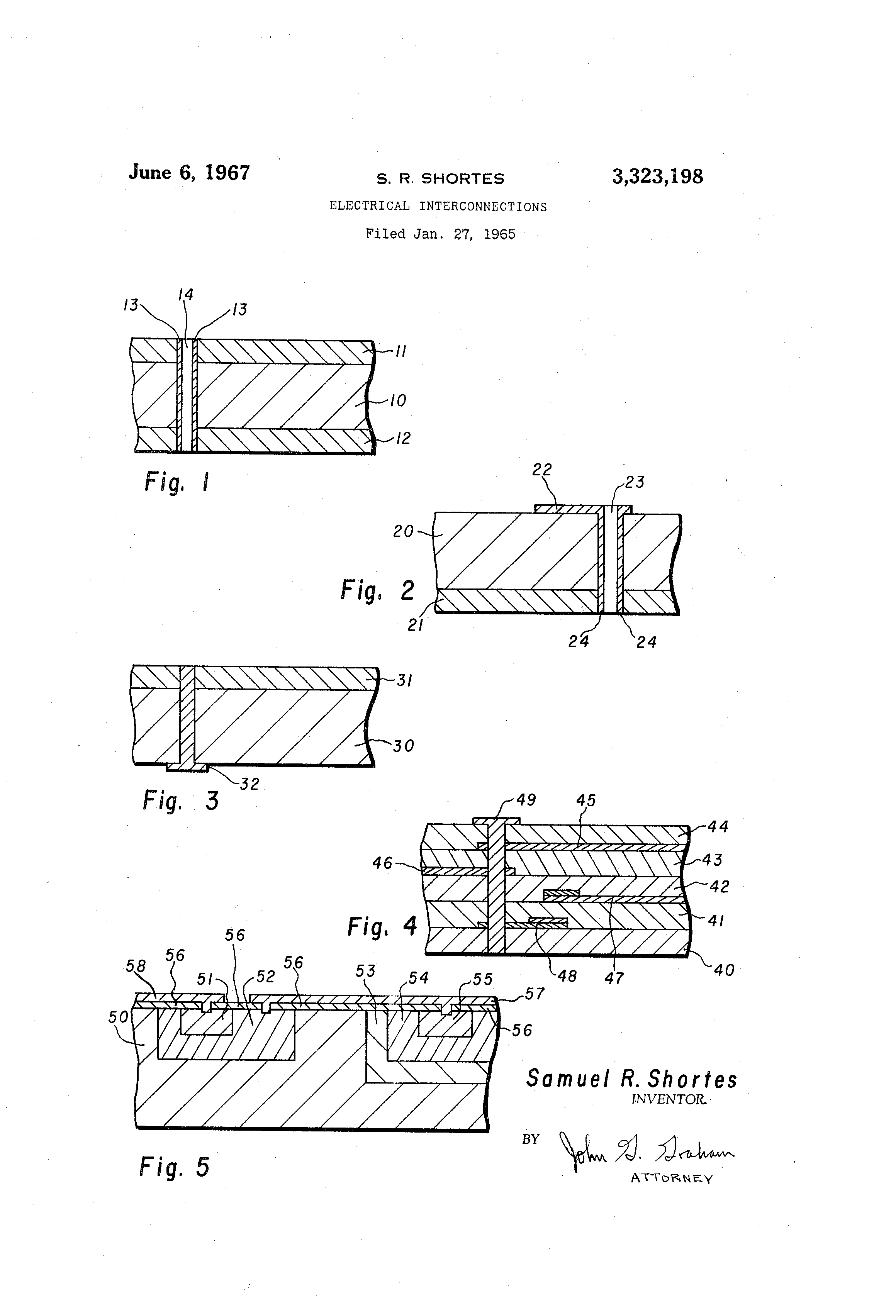
The first patent for through-hole PCB technology in 1967.
The Dawn of the Microprocessor (the 1970s)
The 70s brought us the first microprocessor in the form of an integrated circuit (IC). This was originally developed in 1958 by Jack Kilby at Texas Instruments. Kilby was a newbie at TI, and so his innovative ideas for the IC were largely kept to himself. However, when senior TI engineers were sent out for a week-long conference, Kilby stayed behind to run with the ideas in his head. Here he developed the first IC in the TI labs, and the returning engineers loved it.
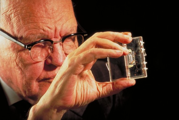
Jack Kilby is holding the first integrated circuit.
It’s in the 1970s where we see ICs first being used in the manufacturing of electronics. By this time if you weren’t using a PCB for connectivity you were in big trouble.
The Dawn of the Digital Age (the 1980s)
The Digital Age brings about massive changes in how we consume media with the introduction of personal devices like the compact disc, VHS, camera, gaming consoles, walkmans, etc.
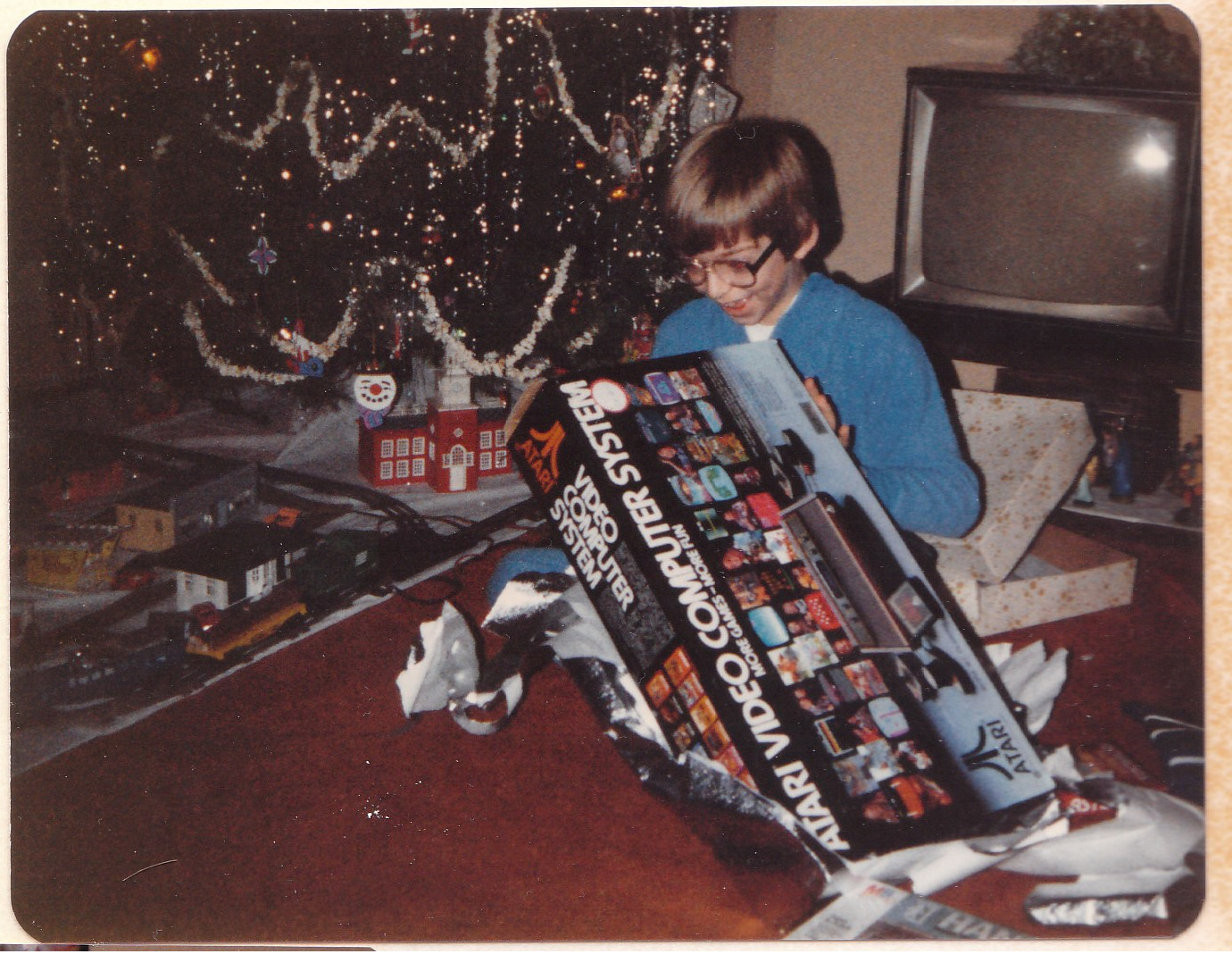
Making a kid’s dream come true with the Atari video game console in 1980.
It’s important to note that PCBs were still being drawn by hand with a light board and stencils, but then computers and EDA arrives. Here we see EDA software like Protel and EAGLE completely changing how we design and manufacturer electronics. Instead of photographs of PCBs, we’re now able to save our designs as Gerber text files whose coordinates can be fed into manufacturing machinery to produce a PCB.
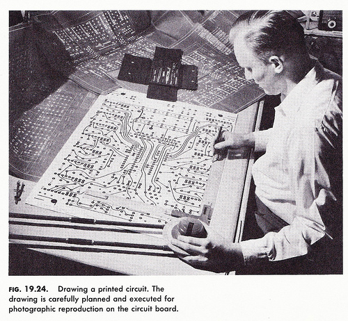
Drawing a printed circuit board with tape and mylar before EDA arrived.
The Internet Age (1990s)
In the 90s we see the use of silicon come into full swing with the introduction of BGAs. Now we can fit more gates onto a single chip and start to embed memories and Systems on Chip (SoC) together. This is also a period of intense miniaturization in electronics. We don’t see any new features added to PCBs, but the entire design process is starting to change and evolve, shifting to the IC.
Now designers have to implement Design for Test (DFT) strategies into their layouts. It’s not as easy to pop off a component and add a blue wire. Engineers have to design their layouts from the perspective of future rework in mind. Are all of those components placed in a way that they can be easily removed? This is a huge concern.
This is also a time where smaller component packages like 0402 make the hand soldering of boards nearly impossible. The designer now lives in his EDA software, and the manufacturer handles the physical production and assembly.
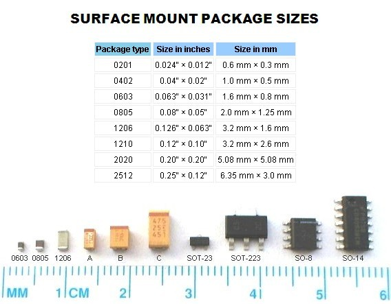
Surface mount components from largest to smallest.
The Hybrid Age (2000s and Beyond)
Cut to the present age of electronics and PCB design; we call this the Hybrid Age. In the past, we had multiple devices for multiple needs. You needed a calculator; you bought a calculator. You wanted to play video games; you bought a video game console. Now you can buy a smartphone and get 30 different layers of functionality built in. This might seem incredibly obvious, but when you really look at everything our smartphones can do, it’s pretty astounding:
| Gaming Device | Address Book | Barcode Scanner | |
| Flashlight | Clock | Camera | Navigation |
| Music Player | Schedule | Video Recorder | Map |
| Internet Browser | Calendar | Movie Player | Calculator |
| Telephone | Note Pad | Tickets | Voice Recorder |
| Answering Machine | Text Message | Banking | Books |
We’re in an age of consolidation of devices, but what’s coming next? PCBs are established, we have processes and procedures for nearly everything. High speed applications are becoming the norm. We’re also seeing only 25% of PCB designers under the age of 45, and 75% is getting ready to retire. The industry seems to be in a period of crisis.
Could the future of PCB design be in robotics? Maybe in wearables with flexible circuitry? Or perhaps we might see protons replacing electrons with Photonics. As for the physical PCBs that we have come to know, even those might change in the future. Instead of needing a physical medium for connectivity between components there is the potential for wave technology. This would allow parts to send signals wirelessly without needing copper.
What Will the Future Hold? No one really knows where PCB design is headed in the future or even electronics as a whole. Nearly 130 years have passed since our manufacturing muscles have kicked into motion. Since then, the world has been forever changed with major introductions like the automobile, electric appliances, computers, smartphones, and a whole lot more. Gone are the days of our reliance on coal, wood, or oil for all of our basic sustenance and survival. Now we have electronics that can power our everyday needs.
But what will the future hold? That’s a big unknown. What is known is that every invention that came before us stood on the shoulders of its predecessor. Our forefathers got PCB design where it is today, and now it’s up to us to innovate and revolutionize how we design and interact with technology. The future could be anything. The future is up to you.
原文地址:https://www.autodesk.com/products/eagle/blog/history-of-pcbs/

